
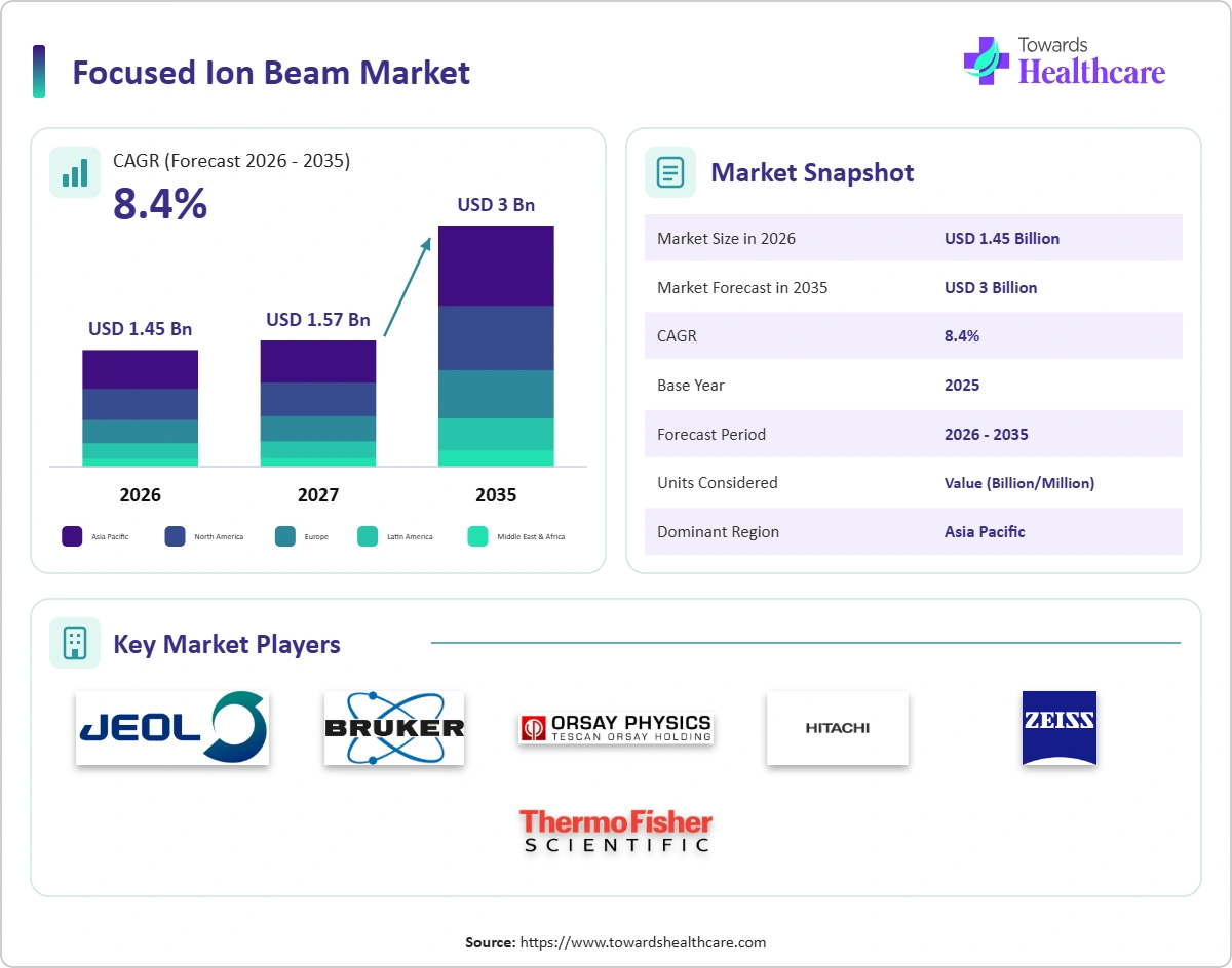
The global focused ion beam market is projected to grow from USD 1.34 billion in 2025 to USD 3.00 billion by 2035, driven by the growing requirement for nanoscale material processing, semiconductor inspection, and advanced imaging technologies. Focused ion beam systems play an important role in semiconductor manufacturing because they enable precise material removal, circuit modification, defect analysis, and preparation of samples for transmission electron microscopy.
The complexity of semiconductor architectures necessitates advanced failure analysis and material characterization techniques. Plasma FIB systems are favored for their efficiency in milling larger samples, while dual-beam FIB-SEM platforms integrate imaging and milling capabilities. In materials science, these platforms serve applications such as battery research and nanofabrication. Furthermore, cryo-FIB is gaining traction in life sciences for sample preparation, cryo-electron microscopy, and tomography.
These developments are expected to increase market revenue to USD 2.01 billion by 2030 and sustain a CAGR of 8.4% through 2035. FIB systems complement electron microscopes and other advanced microscopy platforms across semiconductor manufacturing and research laboratories.
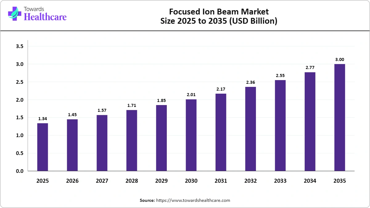
Analyst View: Our market assessment includes focused ion beam systems and services, covering gallium-ion FIB, plasma FIB, and dual-beam FIB-SEM instruments. The estimate considers system installations, average instrument prices, product portfolios, regional semiconductor manufacturing activity, and demand from materials science and life science research. The forecast also incorporates developments in advanced semiconductor packaging, automated sample preparation, cryogenic imaging, and plasma ion beam technology.
| Driver | Impact | ≈ CAGR Contribution | Time Horizon | Key Regions |
| Advanced chips need failure analysis | High | +3.28 pp | Short to long term | Global, strongest in Asia Pacific |
| Advanced packaging grows | Medium | +2.77 pp | Medium to long term | Global, fastest uptake in Asia Pacific |
| Battery and materials research | Medium | +2.36 pp | Short to medium term | Global |
| Cryo-electron tomography | Low | +1.84 pp | Long term | Developed and emerging markets |
Note: Contributions are indicative estimates of each factor's effect on annual growth.
Sources: Expert interviews, secondary sources, Towards Healthcare database and Towards Healthcare analysts.
The focused ion beam market is growing due to advanced semiconductor failure analysis, increasing the need for precise defect inspection and circuit modification. Key drivers include advanced packaging and demand in battery research, materials characterization, and cryo-electron tomography, with an estimated combined gross contribution of 10.25 percentage points to the modelled annual growth rate, before accounting for restraints. Asia Pacific is set to benefit from semiconductor manufacturing investments and advanced packaging expansion, while diverse research markets will drive demand in materials and life sciences.
| Restraint | Impact | ≈ Negative CAGR Contribution | Time Horizon | Key Regions |
| High system costs | High | -0.83 pp | Short to medium term | Global |
| Skilled operator needs | High | -0.61 pp | Medium term | Price-sensitive and emerging markets |
| Long purchase cycles | Medium | -0.41 pp | Short term | Asia Pacific and other mature markets |
Note: Contributions are indicative estimates of each factor's effect on annual growth.
Sources: Expert interviews, secondary sources, Towards Healthcare database and Towards Healthcare analysts.
The model estimates that the identified restraints could offset approximately 1.85 percentage points of annual growth due to high system costs, limited availability of skilled operators, and extended procurement cycles. High equipment prices represent the primary restraint, particularly for smaller research facilities and institutions with limited capital budgets. Despite these challenges, improvements in automation, instrument performance, and service availability are expected to support overall market expansion and sustain a CAGR of 8.4% from 2026 to 2035.
The development of advanced plasma FIB systems presents significant opportunities for manufacturers as semiconductor architectures become more complex. Increasing demand for large-volume milling, advanced packaging inspection, and high-throughput sample preparation is encouraging investment in next-generation plasma ion sources.
Cryo-FIB shows significant growth potential, driven by research advancements in structural biology, cellular imaging, and cryo-electron tomography. Manufacturers can enhance their market position by creating integrated cryogenic sample preparation platforms and automated workflows for life sciences.
The expansion of semiconductor fabrication facilities globally is driving demand for FIB-SEM instruments and services. Automation, AI-driven detection, and advanced imaging software enhance productivity while reducing operator dependency. Moreover, specialized service laboratories are poised to benefit from the rising need for outsourced failure analysis, TEM sample preparation, circuit editing, and advanced material characterization.
Note: 2025 is the base year; 2035 shares and CAGRs are forecasts.
Sources: Expert interviews, secondary sources, Towards Healthcare database and Towards Healthcare analysts.
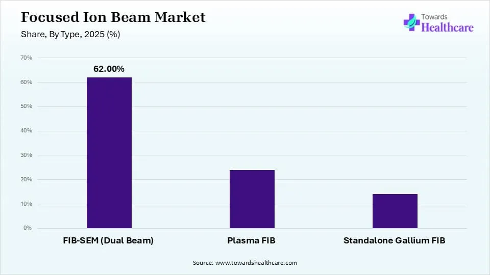
FIB-SEM (Dual Beam) accounted for 62% of the market in 2025 and is projected to expand at a CAGR of 7.73% from 2026 to 2035. These systems combine focused ion beam milling with scanning electron microscopy, enabling users to perform precise material removal and high-resolution imaging. The established use of dual-beam systems across semiconductor manufacturing and research laboratories supports their leading market position, although their growth is expected to remain below the overall market CAGR.
The Plasma FIB use high-current ion sources to enable faster milling and larger-volume material removal than conventional gallium-based systems in suitable applications. The increasing complexity of semiconductor structures and demand for efficient sample preparation are expected to strengthen the segment's growth.
Standalone Gallium FIB systems use gallium ion sources for precise material removal, circuit editing, nanofabrication, and localized sample preparation. However, the expansion of plasma-based alternatives is expected to influence the segment's relative market share.
Segment Outlook: FIB-SEM (Dual Beam) systems are expected to remain the largest type category through 2035, although their share is projected to decline to approximately 58.33%. Plasma FIB is anticipated to record the fastest growth, increasing its share to 28% by 2035. This transition reflects the importance of large-volume milling, advanced semiconductor inspection, and high-throughput sample preparation.
Note: 2025 is the base year; 2035 shares and CAGRs are forecasts.
Sources: Expert interviews, secondary sources, Towards Healthcare database and Towards Healthcare analysts.
Failure Analysis and TEM Sample Prep accounted for 44% of the market in 2025 and is projected to expand at a CAGR of 7.90% from 2026 to 2035. Semiconductor manufacturers use these techniques to investigate process defects, analyze device structures, and improve manufacturing quality. The increasing complexity of semiconductor devices is expected to sustain demand, although the segment's growth may remain below the overall market rate.
Nanofabrication and Circuit Edit FIB-based nanofabrication enables precise modification and patterning of materials at extremely small scales. The growing demand for advanced semiconductor research and device development is expected to support segment expansion.
The 3D Imaging and Tomography FIB-SEM tomography enables high-resolution, 3D reconstruction by sequentially removing and imaging materials, with applications in materials science, semiconductor packaging, battery research, and life sciences. Interest in nanoscale structural analysis and cryogenic imaging is expected to drive the segment's faster growth.
Others category includes specialized research and industrial applications involving material characterization, localized processing, and advanced microscopy workflows. Demand from academic laboratories, nanotechnology research centers, and specialized industrial users is expected to support steady segment development.
Segment Outlook: During the forecast period, Failure Analysis and TEM Sample Prep is expected to remain the largest application, although its share is projected to decline to approximately 41.67%. Meanwhile, 3D Imaging and Tomography is anticipated to record the fastest growth, increasing its share to 24.33%. This trend reflects the growing use of FIB technology in advanced materials characterization, semiconductor packaging, and life science research.
Note: 2025 is the base year; 2035 shares and CAGRs are forecasts.
Sources: Expert interviews, secondary sources, Towards Healthcare database and Towards Healthcare analysts.
Semiconductors and Electronics accounted for 56% of the market in 2025 and are projected to expand at a CAGR of 7.96% from 2026 to 2035. Semiconductor manufacturers use focused ion beam systems for defect analysis, circuit modification, and advanced packaging inspection. The complexity of semiconductor nodes and the rise of 3D integration technologies will drive demand, but market share for this segment is expected to slightly decline due to the growth of other research applications.
Materials Science FIB technologies are utilized for analyzing metals, alloys, batteries, nanomaterials, and advanced composites. They enable researchers to study material interfaces, structural defects, and nanoscale properties. Growing investments in battery technologies and advanced materials research are anticipated to drive segment growth.
Life Sciences increasing use of cryogenic focused ion beam systems for biological sample preparation is strengthening demand across structural biology and cellular imaging. Growing research into cellular structures, protein interactions, and molecular mechanisms is expected to accelerate adoption.
Others category includes specialized applications in academic research, nanotechnology, industrial material inspection, and other scientific investigations. Continued investments in advanced microscopy and materials characterization are expected to support steady demand.
Segment Outlook: Through 2035, semiconductors and electronics are expected to remain the largest end-user category, although their market share is projected to decline to around 53.67%. Life sciences is anticipated to record the highest CAGR of 10.36%, increasing its share to 14.33%. This transition highlights the growing significance of cryo-FIB technology, structural biology, and advanced cellular imaging applications.
Analyst View: Based on our analysis, FIB-SEM (Dual Beam), Failure Analysis and TEM Sample Prep, and Semiconductors and Electronics represent the largest categories in the focused ion beam market. However, Plasma FIB, 3D Imaging and Tomography, and Life Sciences are expected to gain market share as advanced semiconductor packaging, large-volume milling, cryogenic imaging, and specialized materials research expand.
Note: 2025 is the base year; 2035 shares and CAGRs are forecasts.
Sources: Expert interviews, secondary sources, Towards Healthcare database and Towards Healthcare analysts.
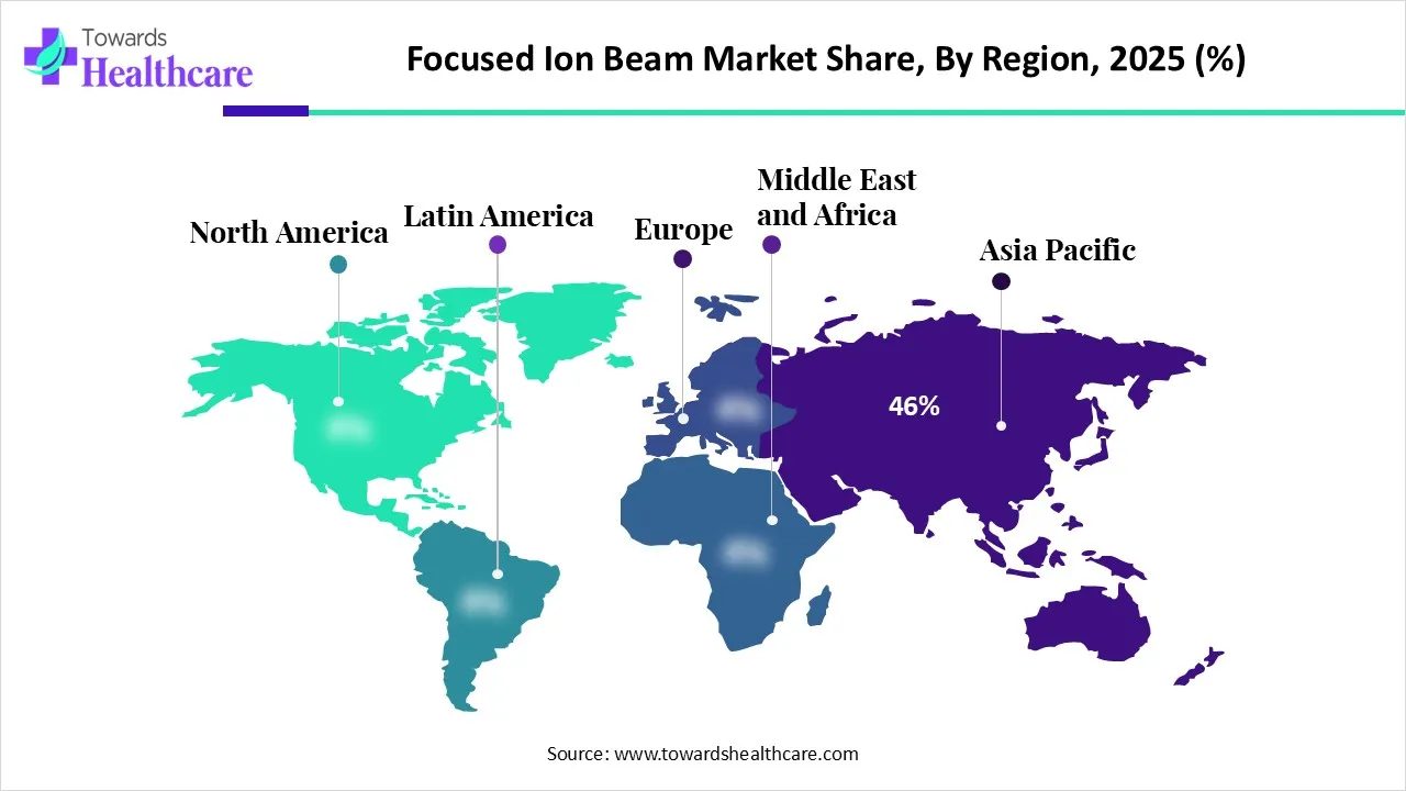
Asia Pacific held 46% of the global focused ion beam market in 2025. The region is projected to register a CAGR of 9.03% from 2026 to 2035. Countries such as Taiwan, South Korea, China, and Japan are major contributors to regional demand. The expansion of semiconductor manufacturing, advanced packaging, and high-density integrated circuits is increasing the need for FIB-SEM systems and plasma FIB technologies. Growing investments in semiconductor research and domestic manufacturing capabilities are also encouraging equipment procurement. Additionally, expanding materials science and life science research is supporting demand for specialized FIB applications. The region's strong electronics manufacturing ecosystem, combined with government-supported semiconductor investment, is expected to strengthen its market position through 2035.
North America the United States leads in regional semiconductor demand due to significant investments in manufacturing, advanced packaging research, and a robust electronics sector. Government backing for domestic manufacturing is anticipated to boost investments in advanced inspection and failure analysis equipment. Canada contributes through research in materials science and technology. However, North America's market share is expected to slightly decline as Asia Pacific experiences faster growth during the forecast period.
Europe market, Germany plays an important role owing to its strong scientific instrument industry and semiconductor research ecosystem. The United Kingdom, France, and other European nations contribute to academic research, nanotechnology, materials characterization, and advanced electronics development. Equipment manufacturers such as ZEISS and TESCAN enhance regional competition, while growing research in advanced semiconductor packaging, battery materials, and cryogenic imaging is anticipated to foster ongoing market development.
Latin America regional demand for semiconductor manufacturing remains limited, but research investments and infrastructure improvements are fostering opportunities in Brazil and Argentina. Growing interest in nanotechnology and battery materials is driving demand from universities and research facilities for FIB systems. However, challenges such as reliance on imported instruments and constrained budgets may hinder the broader adoption of advanced systems.
The Middle East and Africa regional demand is bolstered by investments in scientific research, university infrastructure, advanced materials development, and technology diversification. GCC countries are enhancing their research and innovation capacities via investments in advanced laboratories and technology-focused institutions, while South Africa contributes through materials science and mining research.
Analyst View: According to our analysis, Asia Pacific is set to lead the focused ion beam market owing to its robust semiconductor manufacturing ecosystem and electronics industry growth. North America will maintain a significant market presence owing to semiconductor research investments, while Europe will benefit from established microscopy manufacturers. Latin America and the Middle East and Africa are anticipated to see gradual growth as scientific infrastructure develops.
| Rank | Company Name | 2025 Share (%) | Key Products / Business | Headquarters |
| 1 | Thermo Fisher Scientific | 43.00% | Helios FIB-SEM and plasma FIB | United States |
| 2 | ZEISS | 15.00% | Crossbeam FIB-SEM | Germany |
| 3 | Hitachi High-Tech | 11.00% | FIB-SEM systems | Japan |
| 4 | JEOL | 7.00% | FIB-SEM systems | Japan |
| 5 | TESCAN | 7.00% | Plasma and gallium FIB-SEM | Czech Republic |
| 6 | Raith | 2.00% | FIB nanofabrication | Germany |
| 7 | Applied Materials | 2.00% | Defect review systems | United States |
| 8 | Orsay Physics | 1.00% | FIB columns | France |
| 9 | ionoptika | 1.00% | Ion beam systems | United Kingdom |
| 10 | Bruker | 1.00% | Analytical add-ons | United States |
Note: Company shares are 2025 estimates.
Sources: Company press releases, expert interviews, secondary sources, Towards Healthcare database and Towards Healthcare analysts.
Thermo Fisher Scientific was a leading participant in the global focused ion beam market in 2025, followed by ZEISS at 15% and Hitachi High-Tech at 11%. These companies maintain competitive positions through established instrument portfolios, technological capabilities, and global customer relationships.
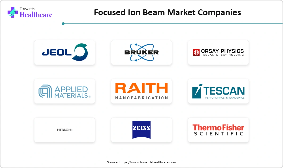
Thermo Fisher Scientific leads the FIB-SEM market with its Helios platforms, supporting semiconductor inspection and analysis. ZEISS offers the Crossbeam FIB-SEM portfolio, while Hitachi High-Tech specializes in FIB-SEM systems for materials and semiconductor research. Other notable companies include JEOL, TESCAN, Raith, Applied Materials, Orsay Physics, ionoptika, and Bruker, contributing to FIB nanofabrication and analytical solutions.
The top 10 companies collectively accounted for an estimated 90.30% of the market in 2025, while the remaining 9.70% was distributed among several specialized ion source, column, component, and technology providers.
Competition in the focused ion beam market is influenced by milling speed, imaging resolution, automation capabilities, plasma source performance, cryogenic functionality, software integration, after-sales service, and equipment pricing. Companies offering integrated FIB-SEM platforms and application-specific solutions are positioned to strengthen their competitive standing through 2035.
Thermo Fisher Scientific: Thermo Fisher Scientific is headquartered in the United States and held an estimated 43% share of the focused ion beam market in 2025. Its product portfolio includes Helios FIB-SEM and plasma FIB platforms used in semiconductor failure analysis, advanced materials characterization, and sample preparation. In the Towards Healthcare Companies Quadrant, the company is positioned as a Leader.
ZEISS: ZEISS, part of Carl Zeiss AG, is based in Germany and accounted for an estimated 15% market share in 2025. Its technological capabilities in electron microscopy and optical systems strengthen its competitive position. ZEISS is placed as a Leader in the Towards Healthcare Companies Quadrant.
Hitachi High-Tech: Hitachi High-Tech is headquartered in Japan and held an estimated 11% market share in 2025. The company's established presence in analytical instruments and semiconductor equipment supports its competitive position. It is recognized as a Leader in the Towards Healthcare Companies Quadrant.
JEOL: JEOL is based in Japan. In 2025, the company accounted for an estimated 7% share of the market. Its product portfolio includes FIB-SEM systems used in materials science, nanotechnology, semiconductor research, and advanced microscopy. JEOL is classified as a Leader in the Towards Healthcare Companies Quadrant.
TESCAN: TESCAN is from the Czech Republic and held an estimated 7% market share in 2025. The company offers plasma and gallium FIB-SEM systems designed for advanced materials characterization, semiconductor analysis, and nanotechnology research. TESCAN is positioned as a Leader in the Towards Healthcare Companies Quadrant.
Raith: Raith is headquartered in Germany and represented an estimated 2% of the focused ion beam market in 2025. The company specializes in FIB nanofabrication and advanced patterning technologies for research and industrial applications. Raith is classified as a Leader in the Towards Healthcare Companies Quadrant.
Applied Materials: Applied Materials is headquartered in the United States and accounted for an estimated 2% market share in 2025. The company focuses on semiconductor manufacturing and defect review systems, with expertise in process technologies to seek opportunities in inspection and materials characterization. Applied Materials is positioned as an Innovator in the Towards Healthcare Companies Quadrant.
Orsay Physics: Orsay Physics is based in France and held an estimated 1% share of the market in 2025. The company specializes in FIB columns and ion beam technologies for scientific instrumentation and microscopy, supporting its role in the focused ion beam ecosystem. It is placed as an Innovator in the Towards Healthcare Companies Quadrant.
ionoptika: ionoptika is headquartered in the United Kingdom and accounted for an estimated 1% market share in 2025. The company focuses on ion beam systems and specialized technologies for advanced scientific research and analytical applications. ionoptika is classified as an Innovator in the Towards Healthcare Companies Quadrant.
Bruker: Bruker is based in the United States and held an estimated 1% share of the market in 2025. Its portfolio includes analytical technologies and related instrumentation that support advanced materials characterization and scientific research. Bruker is acknowledged as an Innovator in the Towards Healthcare Companies Quadrant.
The focused ion beam ecosystem connects upstream ion source and component suppliers with instrument manufacturers, service laboratories, semiconductor companies, research institutions, and funding organizations. Each participant contributes to the development, manufacture, distribution or use of focused ion beam systems across industrial and scientific applications.
| Ecosystem Stage | Role in the Market | Key Companies |
| Component Suppliers | Supply ion sources and columns | Orsay Physics, source makers |
| Instrument Makers | Build FIB systems | Thermo Fisher, ZEISS, Hitachi, JEOL, TESCAN |
| Service Labs | Provide FIB services | Failure analysis labs |
| Users | Analyse and fabricate | Chipmakers, universities, life science labs |
| Funders | Buy for research | Governments, universities |
Sources: Company press releases, expert interviews, secondary sources, Towards Healthcare database and Towards Healthcare analysts.
Component Suppliers: Component suppliers are essential to FIB system manufacturing, delivering ion sources, columns, and specialized components. Companies like Orsay Physics play a key role in developing and supplying these critical components.
Instrument Makers: Manufacturers including Thermo Fisher Scientific, ZEISS, Hitachi High-Tech, JEOL, and TESCAN, develop and commercialize focused ion beam and FIB-SEM systems, integrating ion beam sources, electron microscopy, imaging software, automation, and sample preparation technologies.
Service Labs: Specialized service laboratories provide FIB-based sample preparation, failure analysis, circuit editing, nanofabrication, and materials characterization, enabling clients to access advanced FIB capabilities without investing in a full system.
Users: Semiconductor manufacturers, electronics companies, universities, materials science laboratories, and life science research facilities utilize FIB technologies for sample preparation, imaging, structural characterization, and nanoscale fabrication.
Funders: Governments, universities, and research organizations obtain support for advanced FIB systems through grants and investment programs.
The market value chain begins with upstream ion source and component suppliers. Instrument manufacturers integrate these technologies into complete FIB and FIB-SEM systems, which are distributed to research institutions, semiconductor manufacturers, and industrial customers. Service laboratories provide additional access to specialized capabilities, while government and academic funding supports equipment procurement and technology development. Companies that integrate several stages of this ecosystem or maintain long-term relationships with end users can strengthen their market position.
The Towards Healthcare Companies Quadrant positions key participants in the focused ion beam market by market strength, reflecting revenue scale, market share, and geographic reach, and by innovation and growth strategy, reflecting product portfolio breadth, R&D intensity, and partnerships. Positions reflect each company's estimated 2025 share of the focused ion beam market and our assessment of its product innovation, portfolio breadth, and partnerships.
Sources: Company press releases, expert interviews, secondary sources, Towards Healthcare database and Towards Healthcare analysts.
Leaders: Thermo Fisher Scientific, ZEISS, Hitachi High-Tech, JEOL, TESCAN, and Raith combine high market share with broad portfolios and strong innovation.
Innovators: Applied Materials, Orsay Physics, ionoptika, and Bruker bring newer technologies and specialised products.
By Type
By Application
By End User
By Region
The focused ion beam market estimate is developed using a bottom-up assessment of instrument installations, shipment volumes, average selling prices and demand across major application and end-user categories. The analysis covers gallium-source FIB systems, plasma-source FIB systems and dual-beam FIB-SEM platforms, with each instrument assigned to a mutually exclusive category according to its configuration and ion-source technology. Where included within the market scope, software, maintenance, upgrades and outsourced FIB services are estimated separately to avoid double counting. Regional estimates consider semiconductor manufacturing activity, research infrastructure, instrument procurement, supplier presence and application-specific demand. The 2026-2035 forecast incorporates expected changes in semiconductor architectures, advanced packaging, large-volume milling, automated sample preparation, materials research and cryogenic imaging workflows.
Analyst View: The focused ion beam market is positioned for steady expansion as semiconductor manufacturers and research institutions depend on nanoscale material processing, advanced imaging, and precise sample preparation. FIB-SEM systems will remain dominant, particularly for semiconductor failure analysis and TEM sample preparation, while Plasma FIB is anticipated to capture more market share with advancements in semiconductor packaging. The semiconductor and electronics sector will be the largest end-user, but Life Sciences will witness faster growth owing to the adoption of cryo-FIB technologies. The Asia Pacific region will continue to lead the market, supported by a robust semiconductor manufacturing ecosystem. Opportunities exist in plasma-based ion sources, automated sample preparation, and AI technologies, though challenges such as high equipment costs and export restrictions may hinder growth. Manufacturers offering superior milling performance, imaging accuracy, and automation will likely enhance their competitive stance through 2035.