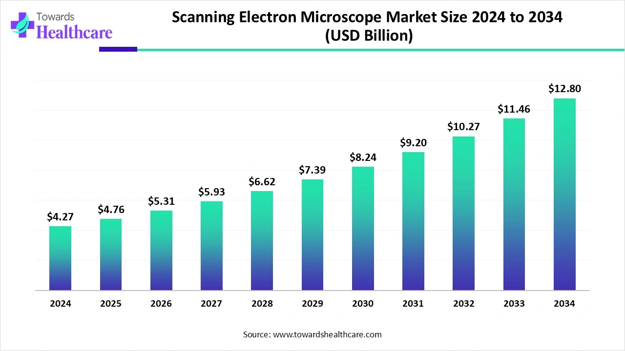
The global scanning electron microscope market size is calculated at US$ 4.27 billion in 2024, grew to US$ 4.76 billion in 2025, and is projected to reach around US$ 12.8 billion by 2034. The market is expanding at a CAGR of 11.64% between 2025 and 2034.
")
The use of scanning electron microscopes in different sectors is increasing for various processes. The growing research and development is also increasing their use, leading to new acquisitions and funding support. AI is also being used to enhance its features, accelerating the optimization processes. At the same time, their use in the development of various novel formulations is also increasing, which is increasing their adoption across various regions. Therefore, to meet with their growing demand, the companies are launching and innovating new SEMs. Thus, this promotes the market growth.
| Table | Scope |
| Market Size in 2025 | USD 4.76 Billion |
| Projected Market Size in 2034 | USD 12.8 Billion |
| CAGR (2025 - 2034) | 11.64% |
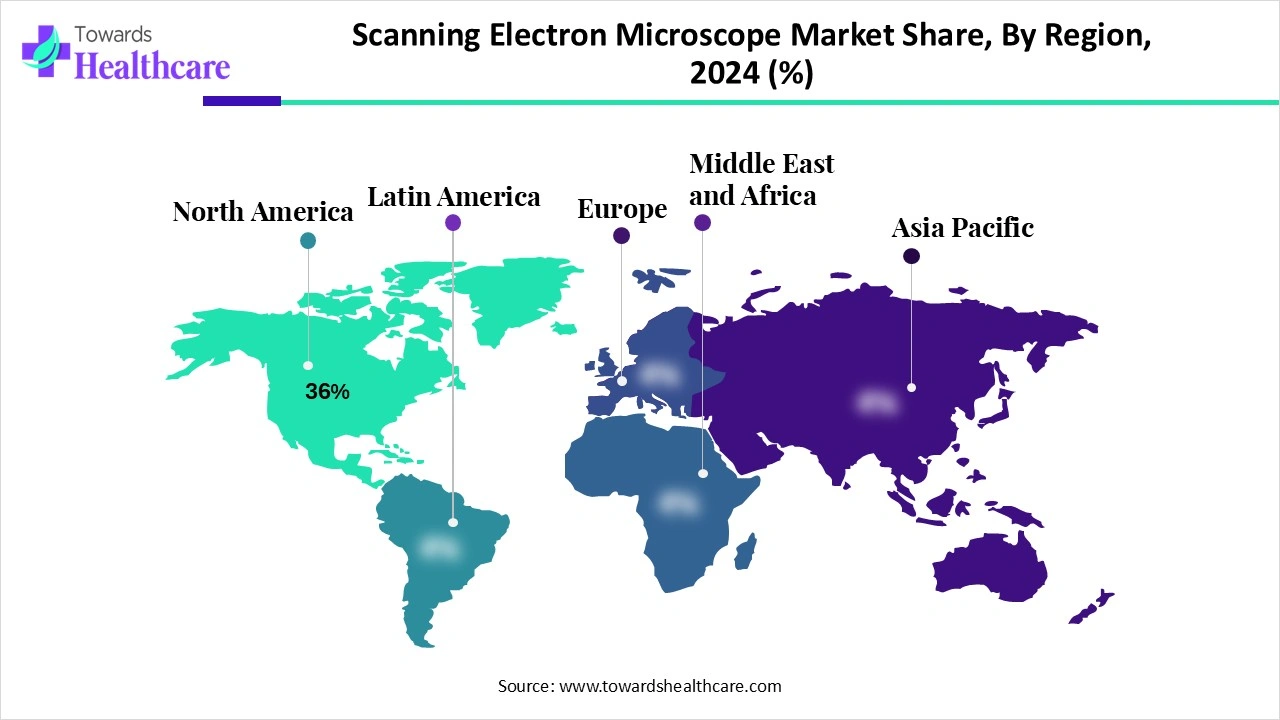
| Leading Region | North America 36% |
| Market Segmentation | By Type, By Technology, By Application, By End User, By Region |
| Top Key Players | Thermo Fisher Scientific, Hitachi High-Tech Corporation, JEOL Ltd., Carl Zeiss AG, TESCAN Orsay Holding, Bruker Corporation, Coxem Co., Ltd., Advantest Corporation, Delong Instruments, Phenom-World (Thermo Fisher), Hirox Co., Ltd., Oxford Instruments, JEOL USA, Inc., Tescan Analytics, Nanoscience Instruments, Nion Co., Tohoku University Instruments (collaborative ventures), Apreo Systems (Thermo Fisher platform), Keysight Technologies (microscopy solutions), Horiba Scientific |
The Scanning Electron Microscope (SEM) market includes advanced microscopy systems that use focused beams of electrons to generate high-resolution surface images of materials at the nanoscale. SEMs are essential tools in materials science, semiconductors, nanotechnology, life sciences, metallurgy, and forensics, enabling researchers to study morphology, composition, and microstructural properties. Demand is driven by rapid growth in nanotechnology, electronics miniaturization, advanced materials development, and biomedical research. The market is characterized by high capital investment, growing adoption of benchtop SEMs for routine labs, and expanding use in industrial quality control.
Increasing research and development: There is a growth in the R&D conducted in various fields, which is increasing the use of SEM for imaging and analysis purposes. Moreover, their growing innovations are also increasing their adoption rates. This, in turn, is leading to new acquisitions and growth in funding to promote their use.
For instance,
The use of AI in the SEM is increasing for automated image analysis as well as for the detection of defects. This helps in accelerating the analysis and interpretation process. It also helps in the optimization of the imaging parameters, which in turn increases the quality of the images. The quality control can be improved due to early and accurate detection of the irregularities or defects in the products with the use of AI. The larger volume of SEM data during the R&D can be interpreted with the use of AI.
Growing life Science Applications
Due to growing life science research and development, the use of SEM is increasing. They are being used for the analysis of tissues, cells, and microorganisms. They are also being used to discover drug interactions and disease mechanisms. Additionally, the growing development of hydrogels and nanoparticles uses SEM for their characterization and analysis of size, shape, and surface morphology. Due to their high resolution and minimal damage to the biological samples, their use in vaccines, novel therapies, and targeted drug delivery development is also increasing. Thus, this is driving the scanning electron microscope market growth.
High Cost and Operational Complexities
The cost associated with the SEM is high. They also require regular maintenance, which adds to the cost. This limits their utilization by small labs or startups. They also require skilled or trained personnel for conducting the procedure and interpreting the results without damaging the samples. Thus, this may limit the use of SEM.
Advancements in the Cryo Scanning Electron Microscope
There is a rise in the use of cryo SEM, which is increasing its innovations. They are used for the imaging of biological samples as they allow high-resolution imaging without affecting or damaging the sample. This is increasing their use across cell biology, tissue engineering, and microbiology fields. They are being used for the analysis of drug crystals, liposomes, and nanoparticles to ensure their stability. They also help in identifying drug interactions, accelerating drug development. Moreover, technological advancements are also enhancing their imaging quality and diagnostic speed. Thus, this is promoting the scanning electron microscope market growth.
For instance,
By type, the conventional/thermionic SEM segment held the largest share of approximately 42% in the market in 2024, due to its easy use. They were widely used for general academic and industrial purposes. Moreover, they were also able to operate under low vacuum and were affordable, which increased their use.
By type, the benchtop/compact SEM segment is expected to show the fastest growth rate at a notable CAGR of approximately 8-9% during the predicted time. As they were cost-effective and have a smaller footprint, they are suitable for routine and teaching labs. It also provided fast results, and simple interface, and automation. This is increasing their use.
By technology type, the conventional SEM segment led the market in 2024, as they were stable and widely used across industries. Moreover, their easy maintenance and durable systems increased their adoption. They were preferred during material analysis, as well as quality control procedures.
By technology type, the field emission SEM segment is expected to show the highest growth during the predicted time. They provide ultra-high resolution, which is increasing their use in electronics and nanotech. Moreover, the growing research and development in life sciences is also increasing their use. Additionally, their stability and surface sensitivity are increasing their use.
By application type, the material science & metallurgy segment held the dominating share of approximately 30% in the market in 2024, driven by increased use in microstructure analysis. They were also used for the analysis of material composition, corrosion, materials fatigue, and defects in metals and their alloys. Moreover, they were also used during quality control and to detect the thermal properties of the materials.
By application type, the semiconductor & electronics segment is expected to show the fastest growth rate during the upcoming years. They are being used for the analysis and imaging of the nanoscale features. They are also used to detect defects or failures in the microchips. Thus, this is enhancing the market growth.
By end user, the academic & research institutes segment dominated the global market with approximately 38% share in 2024, due to growing innovation across multiple fields. Moreover, the growing demand for high-resolution imaging and advanced analytical techniques, increased their adoption rates. Additionally, the government funding also promoted their utilization.
By end user, the semiconductor & electronics industry segment is expected to show the highest growth during the upcoming years. Their use is increasing due to rising demand from chipmakers and nanofabrication labs. Moreover, they are essential for the analysis and inspection of the defects to minimize failures. Thus, this is promoting the market growth.
")
North America dominated the scanning electron microscope market share 36% in 2024. North America consists of a strong academic research base, which has increased the use of SEM. Moreover, due to the growing use of semiconductors, they were also used in the semiconductor industry. The government funding also encouraged their use. Thus, this contributed to the market growth.
The presence of well-known semiconductor, pharmaceutical, and biotechnology industries in the U.S. increased the use of SEM. They are being used for failure analysis, material characterization, and in quality control processes. Moreover, the growing R&D in materials science, life science, and nanotechnology is also increasing its demand. Additionally, the NIH funding is also increasing its adoption rates.
The research and development in the industries and institutions of Canada is increasing, which is using SEM for various purposes. Moreover, the grants and funding provided by the government are increasing the acquisition of SEM. At the same time, their use in the nanotechnology and mining sectors is also increasing.
Asia Pacific is expected to host the fastest-growing scanning electron microscope market during the forecast period. The expanding nanotech, electronics, and academic infrastructure in the Asia Pacific is increasing the adoption of SEM. They are also being used in the automotive and metallurgy sectors for failure analysis and quality control. Moreover, companies are also contributing by manufacturing more affordable and advanced SEMs. Additionally, the government investments and initiatives are driving their adoption rates. Thus, this promotes the market growth.
The R&D of scanning electron microscopes includes integration with AI, improvement of resolution, 3D and in situ capabilities enhancements, and development of new systems and software for promoting automated analysis across various fields.
Key Players: JEOL Ltd., Thermo Fisher Scientific, Hitachi High-Tech Corporation, ZEISS, TESCAN Orsay Holding, Bruker Corporation.
The clinical trials and regulatory approvals of scanning electron microscopes focus on the safety and applications of SEM and their compliance with the quality control guidelines.
Key Players: JEOL Ltd., Thermo Fisher Scientific, Hitachi High-Tech Corporation, ZEISS, TESCAN Orsay Holding, Bruker Corporation, and Danaher Corporation.
The patient support and services of the scanning electron microscopes focus on providing assistance for their installation, training, and sample preparation.
Key Players: JEOL Ltd., Thermo Fisher Scientific, Hitachi High-Tech Corporation, ZEISS, TESCAN Orsay Holding, Bruker Corporation, Oxford Instruments plc.

In October 2024, after receiving the grant for the acquisition of the state-of-the-art Scanning Electron Microscopy-Energy Dispersive Spectroscopy-Electron Beam Lithography (SEM-EDS-EBL) system, the associate professor in the Department of Biological Sciences, Dr. Qunying Yuan, stated that they will be able to move ahead in the multidisciplinary research conducted at AAMU with the use of this one-year grant to acquire an advanced SEM-EDS-EBL system. Thus, new opportunities in fields such as biology, environmental science, electrical engineering, and plant science, along with the military applications, will be provided with this acquisition.
By Type
By Technology
By Application
By End User
By Region

Principal Consultant
Shivani Zoting is a dedicated research analyst specializing in the healthcare industry. With a strong academic foundation, a B.Sc. in Biotechnology and an MBA in Pharmabiotechnology, she brings a unique blend of scientific understanding and strategy.
Learn more about Shivani Zoting
Reviewed By
Aditi Shivarkar is a seasoned professional with over 14 years of experience in healthcare market research. As a content reviewer, Aditi ensures the quality and accuracy of all market insights and data presented by the research team.
Learn more about Aditi Shivarkar